Saturday, December 21, 2019

PROTOTYPE TO PRODUCTION: BUILDING YOUR FIRST PCB PROTOTYPE

This week, we’re excited to kick off a three part blog series about building your first PCB prototype. PCBs (printed circuit boards) are the heart and brains of every product that turns on, plugs in, or lights up. They contain electrical components that determine the behavior of your product, and come in all shapes and sizes. Reference
In this first post, we’re going to share some tips about defining and communicating PCB fabrication specifications, and creating gerber files for your prototype.

WAIT, WHAT ARE GERBER FILES?

Gerbers files are the digital blueprints that allow manufacturers to build your PCB, layer by layer. Many PCB design software packages have built-in tools for generating these kinds of files – at Particle, we use EAGLE, a free and powerful PCB design suite popular with engineers all over the world.
In this blog post, we’re not going to focus on how to create schematics and PCBs in EAGLE, since there are already several extraordinary tutorials on the web that do a great job. In our opinion, this three-part series by ] is among the best:
  1. How to Install and Setup EAGLE
  2. Using EAGLE: Schematics
  3. Using EAGLE: Board Layout
Instead, we’re going to focus on fabrication specifications – the design requirements that have less to do with defining the electrical function of your product, but have a tremendous affect on its cost, yield, supply chain, and manufacturability.
Keep in mind throughout this post that following common manufacturing standards is always the cheapest, fastest, and least complicated route through the prototyping process. The following design rules and standards are often overlooked until the price is too high or the yield is too low, so our hope is that this post will save you some valuable time along the already unpredictable road from prototype to production.

1. UNDERSTANDING PCB FABRICATION SPECS

  • Dimensions – Pretty simple, the size of your PCB. The key thing to keep in mind here is that the cost of a PCB scales with surface area, so be sure to use only the space that you need in order to minimize costs. Similarly, PCB board designs with irregular shapes that result in waste materials during fabrication will be more expensive the a smaller, rectangular footprint for the same board.
relay-shields
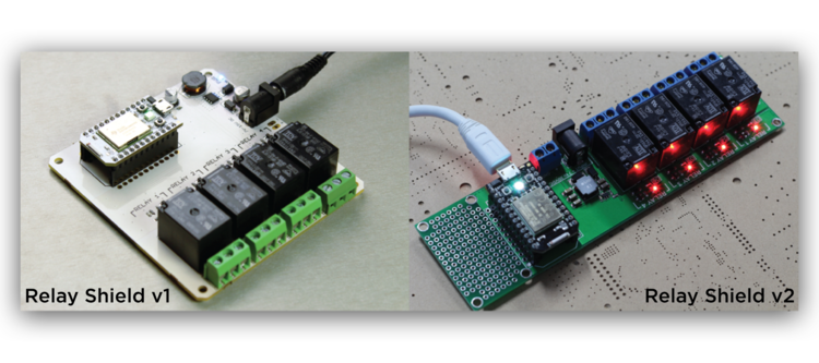
The first version of the Spark Relay Shield has a square footprint of nearly 74.5 cm^2, and lots of unused space. The second iteration (prototype!) has a reduced footprint of only 65.4 cm^2, and includes a large prototyping playground as a bonus.
  • # of Layers – The number of layers in a PCB is a basic indicator of its complexity (lower is simpler). You can think of additional PCB copper layers like highways stacked on top of one another – they provide new planes in which to route the traffic of electrons when the maze of electrical connections between components and pins start to overlap on one another.
  • Material Type – A standard multilayer PCB consists of several copper clad boards fused together on top of each other. The most common type of PCB material used these days is the glass epoxy or more widely know as the FR-4, where FR stands for flame retardant while the number denotes its flammability. About a decade ago, the more commonly used PCB material was the phenolic paper or the FR-2. This material was prone to chipping/cracking and not to mention, more toxic. Other less common PCB materials are polyimide, teflon, PEEK used in flexible boards. Most PCB manufacturers offer FR-4 as a default choice but care must be taken when designing high speed or RF boards where the dielectricity and thickness of the material becomes very important.
  • Board Thickness – This is a primary mechanical specification of your PCB, where 1.6mm thick seems to be the industry standard. Depending on the number of copper layers, the PCB manufacturer will choose PCB core dimensions that result in the desired board thickness. If your PCB is enclosed in a small space, you might desire a thickness like 1.0mm or less. Manufacturers can commonly accommodate thicknesses down to 0.4mm.
  • Plating Finish – Pad plating is a technique in which the exposed copper surfaces of a PCB are plated with another metallic material to improve solderability of the pads during assembly. The most common plating technique is leaded or lead-free HASL (Hot Air Solder Leveling), where solder is pre-applied to the board during PCB assembly. An alternate technique is ENIG (Electroless nickel immersion gold) plating. This is a more expensive plating technique, but offers improved resistance to oxidation and surface planarity (flatness). This makes it a great choice for large BGA components and exposed contact pads or test points.
enig-pcb

The PCB on the left is ENIG plated while the one on the right is standard HASL. Observe how the HASL pads are uneven while the ENIG ones are perfectly flat.

  • Impedance Control – If your PCB has a radio on it (Wi-Fi, Bluetooth, etc.), you may need to specify impedance control. Impedance control means that a set of specified traces (usually the RF net) present a known resistance to all signals traveling within them. Impedance is affected by a variety of factors including the dielectric of the pre-preg material, trace width, and soldermask. Carefully controlled impedance is important for optimizing wireless antenna performance. For example, Wi-Fi antenna circuits are typically controlled to 50-ohm impedance. Impedance control requires expensive equipment, and not all manufacturers are capable of ensuring controlled impedances. Expect this to add to your fabrication costs, and to add more if your tolerances for controlled impedances are relatively strict (< 5% variance from spec. 10% variance typical).
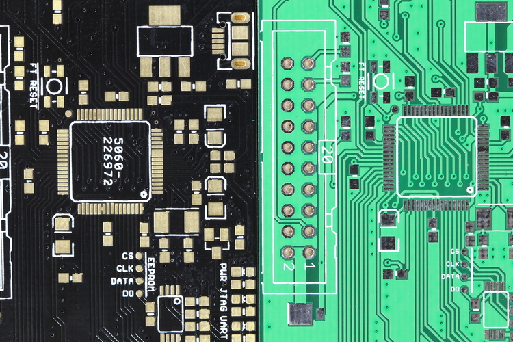
  • Minimum Width/Spacing – This is a measure of the minimum width of the copper traces on your PCB, as well as the minimum distance between individual traces. 6 mil spacing is very safe for most fab houses, while some manufacturers can handle down to 3-4 mil spacing. It’s a great accomplishment to route out 64 or 128 pins of a microcontroller, but only if there’s sufficient spacing to actually fabricate it. So, pick out a spacing requirement that aligns with your manufacturer’s minimum specifications, and stick to it!
pcb-comparison

A board on the left uses default width and spacing tolerances while the one on the right asks for more. Observe how the holes on the vias aren’t exactly centered. This becomes a problem when your PCB manufacturer cannot stick to their tolerances. So try to be more generous with your copper wherever possible.

  • Hole Sizes – The size of the holes and vias (which create vertical electrical connections between copper layers) on your board. Specifying small pads and vias on your PCB is a great way to save space, but also makes it more difficult for your fab house to manufacture. Smaller holes mean tighter tolerances on your manufacturer’s drilling process, a greater likelihood of missing or landing outside the pad, and the creation of scrap and wasted material. 0.2 – 0.3mm vias sizes are typical.
  • Solder mask – A solder mask is a lacquer-like layer of polymer usually applied to the copper traces of a PCB. It helps prevent solder bridges from forming and potentially causing short circuits. Many manufacturers will give you a choice of solder mask color, which is fun! Beyond the standard green, you can oftentimes choose red, yellow, blue, black, or white. Two tips about solder mask selection:
    1. Many quick turn fab houses optimize their manufacturing processes for standard specifications, which include green solder masks. If you want a cheaper, faster turn time, pick green!
    2. White solder masks are awesome and unique, but hard to keep pristine-looking during assembly. The picture below is an example of a pre-production sample of the Spark Core, which occasionally became discolored during high-temperature reflow and wave solder steps. We ultimately chose to switch to a black solder mask in order to avoid the costs associated with cosmetic defects.
photon-discoloration

Pink discoloration (left) on a white soldermask caused by residual chemicals left over from the PCB fabrication process, and agitated by the high heat of reflow and wave solder. Normal sample on the right.

  • Silkscreen – Silkscreens are the final layer applied to your board: the text, graphics, and designators that help to document and annotate your PCB. The correct term for this process is actually “legend printing”, but everyone calls it the “silkscreen” because silk screen printing with epoxy ink is the most common method for creating PCB legends. A more accurate alternative to silk screen printing is LPI printing (Liquid photo imaging) which creates a much higher resolution silkscreen at a slightly higher price point.
silkscreen-comparison

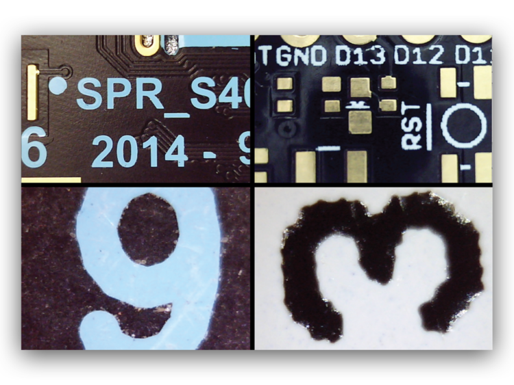
Comparison of LPI (left) versus traditional silk screen legend printing (right) at equal magnification.

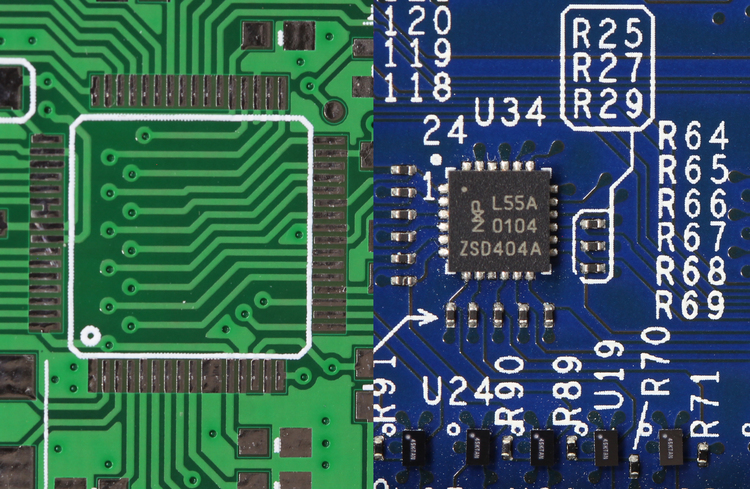
  • Minimum Pitch – In the world of PCBs, “pitch” refers to the distance between adjacent pins on an electrical component. If your product requires a complicated part with lots of pins and a very fine pitch, your manufacturing options may be limited to higher cost assembly houses with modern equipment. Aggressive pitch requirements often result in decreased yield, so it’s reasonable to add the projected cost of scrap (expected scrap rate % * scrap cost) to the price of whatever component is driving the complexity of your PCB. A 0.3mm minimum IC pitch seems to be common for most standard PCB assembly houses.
integrated-circuit.jpeg

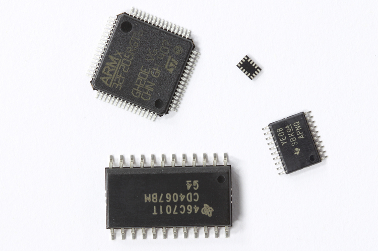
Modern integrated circuits are now available in almost indefinite number of packages and pitches. The QFN and BGA packages tend to be more challenging when prototyping or hand assembling the boards.

  • Castellated Holes – If you’re making a module or PCB that mounts to another PCB, you might consider adding castellated pads to your design. Castellated holes are essentially vias or thru holes that have been cut down a diameter to expose copper along the side face of the PCB (see the picture below). These are super useful in particular use cases, but not all manufacturers can build PCBs with castellated holes, so make sure to do your research.

Tuesday, November 19, 2019

PCB Prototype

If you need prototype printed circuit boards, it's important to work with an assembler who can turn your designs around fast. These boards help verify you have the right design before you start a full production run so you can avoid costly errors. The sooner you get your prototype circuit board back, the sooner you can test it and get started on your standard production run. PCBCart is the PCB manufacturer with fast reaction. We offer quick-turn PCB prototypes to turn your prototype boards around fast while still maintaining complete adherence to your design specifications. Reference

PCBCart offers rapid PCB prototyping services for quick-turn PCB at high quality and low cost. We're fully compliant with quality management systems, and we have an in-house quality control department to verify that all work meets each regulation depicted by the high standards.

Depending on your custom requirements, we can prototype your PCB within 3-7 days, compared to 6-18 days of Standard PCB service. Check out our circuit board prototype capabilities in the following table:

Prototype PCB Service vs. Standard PCB Service
Use PCB Prototype service when you want:


• Boards for Design Review or Preproduction Quality Testing

  Our PCB prototype service is the perfect way to make sure there are no errors in your design before moving into mass production.


• Rapid PCB Turnaround

  Rapid PCB prototyping means you get your boards fast.


• Boards with Eight or Fewer Layers

  Because we are trying to get your boards back to you as fast as possible, we offer rapid PCB prototyping for boards with no more than eight layers.


• FR-4 Boards

  Your printed circuit board prototype will come on standard FR-4 material.


• Quality Standard IPC1 Boards


Use Standard PCB service if you need:


• Boards for Full Production

  Once you know that your design works, you can contact us for standard PCB service for full production for use in your applications.


• Slightly Longer Turnaround Time

  Since these are the boards you will actually be using, it takes a little longer to make sure we get everything just right. However, now that you have tested the design, you can go right into your projects once you get your boards.


• Boards with Up to 9-32 Layers

  We have much more flexibility with materials and layers once we have the time to develop your full boards.


• FR-4, Aluminum, Flex or Other Special Types of Boards

• Quality Standard IPC2 Boards


Refer to this handy chart for a complete breakdown of the differences between our circuit board prototype and standard circuit board services.

What Are the Benefits of Circuit Board Prototyping?
We recommend you PCB prototyping service for function testing of new products prior to making a commitment to a full-production run. Benefits of developing PCB board prototype include:


• Rapidly test and correct designs if there is any mistake

  After waiting over a week for your full boards, you’ll be eager to get them going in your applications. When you test your design beforehand with PCB prototypes, you can do just that.


• Potentially detect any design flaw in the early stages of your projects

  The time to find out mistakes in your design is not when you have a full production run in your warehouse. PCB prototyping service allows you to spot any design problem in a few days, make adjustments and perfect the design before ordering your full run.


• Order low-quantity production runs featuring a MOQ of only five boards if necessary

  Save money and reduce risks by putting off your big orders until you know you have the type of boards you want.


• Benefit from lower production tolerances

  It offers a clear indication of how well your PCB will perform.


Once your proto boards have demonstrated their ability to meet your quality and performance requirements, you are ready for a full production run. Then we will transition from PCB prototype board service to Standard PCB service, which provides tighter production tolerances and more advanced options, including a free Design for Manufacture (DFM) check that is capable of detecting potential issues that could reduce the quality of your PCB.


While it may be tempting to simply order your full printed circuit boards and decide you’ll deal with all design flaws that arise as they come, it’s rarely the most efficient solution. You may get the boards out sooner, but if something goes wrong, it could prove to be a lot costlier and more time-consuming than taking an extra few days to test a prototype.

Save Time and Money in the Long Run With PCB Rapid Prototyping Services from PCBCart
PCB prototyping is the best practice method used world-wide to verify the quality of a design before proceeding. In the past, some companies may not have had time to develop a prototype PCB, wait for the assembler to put that PCB prototype together and then test it. However, thanks to the rapid PCB prototyping offered by PCBCart, this is no longer an issue. You can send in your prototyping PCB board design and have a fast PCB prototype in a week or less, giving you plenty of time to test your PCB proto board to fully prepare for your regular production run.

Get an Instant PCB Prototyping Quote Now
Ready to order prototype PCBs? Click the below button to try our online PCB Prototype calculator, which allows you to independently generate a quote for your custom PCB prototyping project in seconds.

through hole pcb assembly service

Monday, November 4, 2019

What is a printed circuit board?

Computers, machines and other products contain printed circuit boards. These are often colored green and provided with different colored components. A printed circuit board is made of plastic, epoxy or fiberglass. A printed circuit board can be provided with a trace pattern on one side or on both sides. This trace pattern is a printed wiring. These tracks are also called copper or current paths. The tracks are applied to the plate by means of milling and etching.

A bare printed circuit board contains spots, these are the holes on the power lines in which the components must be placed. The components of a printed circuit board are soldered on the other side of the printed circuit board. As a result, a printed circuit board has a current side and a component side. A printed circuit board that is not yet provided with components is called a bare printed circuit board.

Components on a printed circuit board
The components on a printed circuit board are different. These components differ in shape, size and color. The operation of the components also differs from one another, the components all respond differently to electrical current or the electrons. A number of examples of components on a printed circuit board are the capacitor, the diode, an LED, thyristor, zener diode, IC, resistor and the transistor. A number of the aforementioned components of a printed circuit board are briefly explained below.

A resistor often has a small size. Therefore, the value of the resistor is indicated in colors. This color code is in color rings. Every color has its own value.

A diode is also a component that can be placed on a printed circuit board. A diode is a semiconductor and is made from silicon and germanium. The conductivity can be determined with a semiconductor.

A transistor is an important part of an electronic circuit. A transistor can be used as a switch but can also serve as an amplifier. There are different types of transistors with various applications.

An IC is an abbreviation that stands for Integrated Circuit. This is integrated in Dutch. These are applied in various ways.

Accurate work
Making a printed circuit board is very precise work. The trace pattern must be determined and the resistances must be accurately soldered to the plate. If this is not done carefully, parts of the printed circuit board may not work or the entire pin board cannot be used. In addition to making a printed circuit board, placing a printed circuit board in a machine is also precise work.

Get more details: 

Thursday, October 10, 2019

How to Select Material for Your PCBs from Cost and Reliability Considerations

Material, usually substrate material as far as PCB (Printed Circuit Board) is concerned, plays a core role in PCB since it carries its leading functions and properties. Besides, PCB material allows PCBs to conform to some high and special requirement set by the products or projects they’ll work for. Furthermore, it is beneficial to reduce cost and improve products’ reliability when optimal material is selected.


Elements to be Considered in PCB Material Selection
• Glass Transition Temperature (Tg)

Tg refers to the temperature at which material is converted into glass state. Standard Tg stays above 130℃ while high Tg above 170℃ and mid Tg above 150℃.

When it comes to material for PCBs, high Tg should be picked, which should be higher than the working temperature current runs.

• Coefficient of Thermal Expansion (CTE)

As the temperature of substance rises, substance will suffer from expansion or shrinking. When it comes to PCB fabrication, since CTEs in X, Y and thickness are different, PCB will tend to become deformed. Furthermore, plated hole may suffer from breakage or components will get damaged. Therefore, CTE of substrate material should be sufficiently low. pcb assembly illinois

• Heat Resistance

PCB is required to be heat resistant. Generally speaking, PCBs should feature heat resistance of 250℃/50s, which also works on material.

• Flatness

PCB is required to feature excellent flatness. As far as SMT assembly is concerned, PCB is required to feature warpage lower than 0.0075mm/mm.

• Electrical Performance

High-frequency circuits call for PCB material with high dielectric constant and low dielectric loss. Besides, insulation resistance, dielectric strength and Arc resistance should be compatible with product requirement.

Correlation between PCB Material Selection and Product or Industry
PCB material selection plays a decisive role in contributing to product reliability and is also determined by industry particularity and requirement.

Commonly-used electronic products call for FR4 epoxy fiber glass substrate. After all, the products don’t call for special requirement on flexibility, temperature and density.

Electronic products calling for higher requirement on environmental temperature or flexibility, polyimide glass fiber substrate is applied. For high frequency, PTFE glass fiber substrate should be applied. For PCBs calling for higher requirement on thermal dissipation, metal base substrate should be used.

Classification of PCB Substrate Material
https://soundcloud.com/user-504271600
http://guildwork.com/users/absolutepcb
https://myspace.com/absolutepcb
https://data.world/absolutepcb
https://maptia.com/absolutepcb
https://coub.com/absolutepcb
https://www.veoh.com/users/absolutepcb
https://www.appfutura.com/companies/absolute-pcb-assembly
http://addpoll.com/absolutepcb
https://www.cheaperseeker.com/u/absolutepcb

Sunday, September 15, 2019

PCB Assembly

When you design a prototype circuit board, there are a few general rules that you must follow to ensure that the entire PCB manufacturing process runs smoothly. Here we have collected some tips and tricks that will help every beginner for PCB assembly.

Placing components

There are three main types of prototype PCB assembly, single-sided, double-sided and multi-layered. Each type of board has different rules for each of their components, but as a rule of thumb it is always a good idea to place components at the top of the board. It is important to place all components at their specific locations, including switch connectors, LED, mounting holes or heat sinks.

The aim is to minimize the track length between components to ensure that the prototype circuit boards do not cause a short circuit. Easily put parts that are connected to each other next to each other, and it will be easier to lay the tracks on the road.

ICs may only be placed in one place on the board, up and down or from left to right. Doing more than this can cause confusion in the circuit of the board. You also save a lot of time if you leave enough space between these components, because the tracing lines must go between them.


Placing
soil and force tracks After soldering the components, the next step is to lay the force and soil tracks. The power and ground lines are essential when working with the IC, because they are connected to common rails for each power supply. This is a way to prevent daisy-chaining power lines from part to part.

Placing signal tracks
The purpose here is to make the signal tracks as short and as direct as possible. Pass-through holes, called vias, can move signals from one layer to another, so use them to your advantage. Tracks carrying a larger current must also be wider than all other signal tracks to prevent short circuits.

Get more details: pcb assembly illinois 

Monday, August 12, 2019

Guide : How to repair a Motherboard


The motherboard is the control point of a smartphone. With a defective motherboard, a smartphone
performs poorly or not at all. All essential parts are connected to the motherboard. Consider the
touchscreen, audio, charging and power ic chip.
Today we use our smartphones and tablets a lot. The chance that the motherboard will be damaged
by a fall or impact is very high. A defective motherboard is very annoying because it plays the most
important role in making a smartphone work. In most cases, data can be retained during a
motherboard repair. We offer motherboard repairs for products from the following brands: Apple,
Samsung, HTC, Huawei, Sony, Nokia / Microsoft, LG, One Plus & MacBooks.
Make an appointment now for a motherboard pcb assembly illinois. We repair motherboards within
1 to 2 business days. Our motherboard repairs are carried out at our location in Rotterdam. Are
you unable to visit our office in Rotterdam? Send your device!

Touchscreen connector repair

A moderate or non-working touchscreen can be the result of a defective touchscreen connector.
We use high-quality touchscreen connectors. Phonedokter repairs touchscreen connectors within
1 to 2 business days. Make an appointment now and have the damaged motherboard repaired at
our location in Rotterdam.

LCD connector repair

Does the screen of your device stay on? Is the screen colored red? The LCD connector may be
damaged. A motherboard repair can solve the problem. There is also the case that the LCD screen
is broken. A screen repair would be a solution in that case. Make an appointment for a repair now.

Battery connector repair

The battery connector ensures that the motherboard is connected to the battery. When the battery
connector is broken, the device is functioning poorly or not at all. We repair a battery connector
within 1 to 2 business days.

Motherboard wifi repair

Do you have a lost WiFi connection? Or is the device not connected at all to WiFi. The Wi-Fi chip
may be damaged. A WiFi motherboard repair can correct this problem. We repair this part within
1 to 2 business days.

Motherboard sim card reader repair

With a defective SIM card reader, you can no longer make calls or receive phone calls. Symptoms
that show that a device needs a SIM card reader repair are: SIM card registration failed. The
network signal is automatically switched on and off regularly. The pins in the SIM card reader are
damaged or missing. 
Do you experience this type of problem? Has the SIM card reader of your device repaired?

Motherboard charging connector plug repair

Does your device have problems while charging? A broken charging cable can be the cause. Try
using a new and original cable. If the problem still occurs, the device's charging connector plug
may be broken. Phonedokter repairs a charging connector plug within 1 to 2 business days.

Motherboard backlight repair

With a damaged backlight, a device has little image contrast. We can replace the backlight circuit.
Our experienced technicians repair the motherboard professionally and quickly.

Motherboard power ic chip repair

An unprotected voltage fluctuation can damage the power ic chip. To prevent problems of this kind,
it is essential to use only original chargers. With a defective power ic chip you can say the following:
charging is not possible, the battery is not fully charged, battery drains quickly and/or the device
gets a hot backside quickly.

Motherboard audio chip repair


Does your device have no sound anymore? Chances are that the audio chip is broken. Phonedokter
professionally and quickly repairs motherboards. Make an appointment now for a repair or send your
device!

Sunday, July 14, 2019

10 Top Tips for Working with Printed Circuit Boards

A lot of people who are new to electronics often find themselves intimidated by soldering and working with printed circuit boards (PCB). You needn’t be. Circuit boards are not nearly as fragile, “high-tech,” and complicated as they superficially appear. The process of working with them can be very straight-forward, as long as you follow some simple preparations, procedures, and precautions.

More on PCBs


Skill Builder: Fabricating Project Boxes from PCB Cladding

Circuit Skills: Circuit Board Etching
Different Types of Circuit Boards

We’ve covered the basics of soldering countless times here on Make:, so we won’t touch on that here. What follows is a collection of tips and tricks for working with PCBs beyond just soldering the components (called “populating”) onto the board. Some of these are basics that are too often missed, others are more advanced trickery. Hopefully, they will all be helpful, whether you’re a newbie or a seasoned wirenut.

When you first get into electronics and start putting together kits, those kits usually come with a components check list and each step in the build process is designed to be ticked off as you progress through the project instructions. You are always highly encouraged to inventory all of the parts in the kit before you start and to mark off each step as completed. This is a great habit to never get out of. A lot of the perceived complexity of electronics work is thanks to lots of tiny little parts to track and dozens (and dozens) of solder joins to lay down onto a tiny and over-populated PCB. By just being careful, methodical, and organized, you alleviate a lot of the problem. Taking the time to set up a PCB project, inventorying and sorting the parts into temporary parts bins or bags, reading through all of the instructions, and sort of blocking out the build in your head will all pay off in the end.

pcb box build assembly services


When you first get into electronics, it seems counter-intuitive that you have to expose your circuits to cleaning solutions, but cleaning your PCBs should always be part of your circuit-building regimen. And you want to clean the board before you populate it and after. Make: contributor Ross Hershberger writes: “Cleanliness is next to solderliness. Freshly scrubbed copper takes solder with less heat and wets more thoroughly, so always scrub or otherwise de-oxidize your boards before soldering. I use isopropyl alcohol and a fine abrasive like a Scotch Brite. Or a pen eraser followed by alcohol. For bad corrosion, use a glass fiber “pen.” Steel wool may leave fibers that can cause shorts.” Here’s a brief piece on Maker.io about options available for board cleaning, but in the end, for most of us, it comes down to using rubbing alcohol and the exes’ toothbrush.

Populate Lowest to Highest
PCBs can be very tightly populated on a board and can soon become very crowded, leaving you with little room for getting your components, your iron, and your solder wire to the area where they are needed. One way of improving your board-soldering mojo is to plan how you’re going to populate the board beforehand. Solder on your components, across the board, starting with the lowest (usually the resistors) and moving up. That way, big components won’t get in the way when you’re trying to install low-lying ones right next to them.

Use a Pair of Tweezers
Get yourself a pair of electronics tweezers. Even if you’re not mainly working with surface-mount components, which are tiny enough to require such tweezers, adding through-hole components to the board is much easier with tweezers than trying to get parts in place with your fat and meaty end-effectors.

Use a Component Lead Tool
Component lead bending tools, often branded by a supplier and given away as swag, are a great little addition to your electronics toolbox. Along with pre-planning and organizing, having the discipline to keep your circuits neat, tidy, and tight to the board, will pay off in the end. Precisely bending component leads to the proper lead width can help in that process.

Monday, June 10, 2019

Have a look at the functions of PCB!

PCB will be used wider because it has a lot of advantages, mainly used in PCB assembly Indiana, some of its distinctive features are as follows:


High density. 

For decades, high density PCB with IC integration and installation technology for progress and development.

High reliability. 

Through a series of inspections, testing and ageing test ensures that the PCB lasts longer (usage period, generally 20 years) and reliably works.

Can be designed. 

The properties of the PCB (electrical, physical, chemical, mechanical, etc) requirements can be achieved through design standardization, such as printed circuit board design, time is short, high efficiency.

Can be more productive. 

The use of modern management, standardized size (volume) and automation of production and product quality consistent. PCB assembly Indiana is very popular and produces some of the best and high-quality PCB circuit boards that are reliable and more productive.

Testability. 

Establish a relatively complete test method, test standards, test the equipment and instruments to detect and identify PCB products, such as eligibility and service life.

Can be mounted.

Standardized assembly PCB products, both for the various parts, and can be automated, large-scale production. Meanwhile, PCB and components assembled components can be assembled into larger components, systems, up to the machine.

Maintainability. 

Due to PCB and component subunits, it is on the standardization of the design and size of the production, so these parts are standardized. So once the system error, can be replaced quickly, easily and flexible, fast repair service systems work. Of course, you can do more, for example. Such as miniaturization, lightweight, high-speed transmission signals, and so on.

Also read: How do you save a printed circuit board?

Name: Absolute Electronics Services LLC
Address: 2410 Elmhurst Rd Elk Grove Village
Phone:  +1(224) 366-0290

http://c4uc.org/User-Profile/userId/8763.aspx
https://meld.de/profile/absolutepcb?tab=profile
https://www.bagtheweb.com/u/absolutepcb/profile
https://yourlisten.com/absolutepcb
https://torgi.gov.ru/forum/user/profile/734059.page

Wednesday, May 15, 2019

Here are some advantages of a flex printed circuit board | Absolute Electronics Services LLC

What You Should Know About Flex Printed Circuit Boards

Flexible circuit boards were originally designed as a replacement for traditional wire harnesses. From early applications during the Second World War 2, to the present, growth and distribution of flex circuits and flexible printed circuit boards remains exponential.


The Benefits Of Flexible Printed Circuit Board Manufacturing

Electronic devices have taken on a prominent part of our daily lives. The extensive range of servers regardless of their size and use of mobile phones are now being designed to be flexible, lightweight and efficient. While they all come in different shapes, sizes and functions, there is one thing in common - they include flexible printed circuit boards.


Advantages Of Using The Flex PCBs


Flexibility - the most prominent advantage.


The elastic nature of the rapid PCB prototyping in Illinois flex allows placement around the edges and folds.

The flexible nature of the flex printed circuit boards is used in the electronic devices that require 3 axis connections.

Very little or no wiring is required that eliminates wire connection error and increases device reliability.


Space and weight saving

Flex PCBs store up to 60% of the weight and space compared to rigid PCB or wire harness applications.

Bending cycles

Flex PCB use in 3D designs eliminates connecting lines, while the number of bending cycles can be as much as 200,000 (with standard material)


Benefits of the anti-vibration

Additional flexibility and lighter weights allow the flex circuits to absorb and reduce the impact of vibrations on themselves as well as all joints of the solder connections.


Use in a harsh environment

Flex circuits can be built with materials suitable for use in harsh operating environments (materials that have the following properties: waterproof, moisture proof, shockproof, high-temperature oil, corrosion resistant)

Consistent thin inner layers


Heavy copper layers


Heavy copper layers can be used for powerful applications with thin copper layers for flexibility.

There are rapid PCB prototyping in Illinois that have done a remarkable job in the field of flex printed circuit boards. One of them is Absolute Electronics Services LLC, visit their website to know more about the latest in the field.


Name: Absolute Electronics Services LLC

Address: 2410 Elmhurst Rd Elk Grove Village


Also read: Get to know a little about Aluminium PCB


https://forum.odroid.com/memberlist.php?mode=viewprofile&u=32967

http://forum.melanomainternational.org/mif/memberlist.php?mode=viewprofile&u=6003